

Packaging
Overview
Semiconductor technology is constantly shrinking in size while growing in capability and functional integration. In order to enable next generation silicon technologies, semiconductor packages have also evolved to provide improved performance and flexibility. Using small form factor packages with Microsemi’s new higher density FPGAs like PolarFire, SmartFusion2 and IGLOO2 devices enables opportunities for innovation throughout the electronics industry.
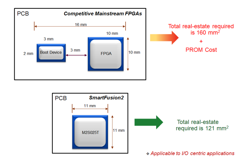
Microsemi’s true flash based FPGAs do not require external configuration memories that are typically required for SRAM based FPGAs. SRAM configuration memories typically are available in 8 pin or 16 pin SOICs’. These devices consume an additional 30mm^2 to 100mm^2 of additional PCB real estate depending on device selected. In addition Microsemi FPGAs do not need to be power sequenced hence saving the additional cost of developing a power sequencing solution and the subsequent recurring costs of additional silicon.
Smallest Form Factor Solutions
Packages
FPGA and SoC FPGA Small Form Factor Packaging
| PolarFire FPGAs | ||||
|---|---|---|---|---|
| Type (Size, Pitch) | MPF100T | MPF200T | MPF300T | MPF500T |
| FCSG325 (11x11, 0.5 mm) | Yes | |||
| FCSG325 (11x14.5*, 0.5 mm) | Yes | |||
| FCSG536 (16x16, 0.5 mm) | Yes | Yes | ||
| FCVG484 (19x19, 0.8 mm) | Yes | Yes | Yes | |
| FCG484 (23x23, 1.0 mm) | Yes | Yes | Yes | |
| FCG784 (29x29, 1.0 mm) | Yes | Yes | Yes | |
| FCG1152 (35x35, 1.0 mm) | Yes | Yes | ||
| IGLOO2 FPGAs | |||||||
|---|---|---|---|---|---|---|---|
| M2GL005 | M2GL010 | M2GL025 | M2GL050 | M2GL090 | M2GL100 | M2GL150 | |
| FCS325 (11x11 mm) | Yes | Yes | Yes | ||||
| VF256 (14x14 mm) | Yes | Yes | |||||
| VF400 (17x17 mm) | Yes | Yes | Yes | Yes | |||
| FCV484 (19x19 mm) | Yes | Yes | |||||
| SmartFusion2 SoC FPGAs | |||||||
| M2S005 | M2S010 | M2S025 | M2S050 | M2S090 | M2S100 | M2S150 | |
| FCS325 (11x11 mm) | Yes | Yes | Yes | ||||
| VF256 (14x14 mm) | Yes | Yes | |||||
| VF400 (17x17 mm) | Yes | Yes | Yes | Yes | |||
| FCV484 (19x19 mm) | Yes | Yes | |||||
Ultra Low density FPGA small form factor Packaging
| IGLOO nano FPGAs | |||||
|---|---|---|---|---|---|
| AGLN010 | AGLN020 | AGLN060 | AGLN125 | AGLN250 | |
| UC36 (3x3 mm) | Yes | ||||
| QN48 (6x6 mm) | Yes | ||||
| QN68 (8x8 mm) | Yes | ||||
| UC81 (4x4 mm) | Yes | ||||
| CS81 (5x5 mm) | Yes | Yes | Yes | Yes | |
Microsemi IC packaging technology efficiently supports high density FPGAs with large pin count Ball Grid Arrays (BGAs), but is also flexible enough to accommodate stringent form factor requirements for Chip Scale Packaging (CSP). In addition, Microsemi offers a variety of packages designed to meet your most demanding application and economic requirements for today's embedded and mobile systems.
Microsemi's Packaging Technology Solution contains helpful information such as technical package details, discussions on the latest environmental issues, related industry articles and links, and implementation tools to assist you with your next design.
Lead-Free "Green" Packaging
![]() The use of lead and other harmful compounds in commercial and consumer electronic devices is a growing environmental problem. As political pressure over health issues have come to bear, the electronics industry has enacted sweeping initiatives to reduce lead in its products. There are many challenges associated with this transition, and Microsemi has dedicated some of its most experienced resources to develop lead-free solutions.
The use of lead and other harmful compounds in commercial and consumer electronic devices is a growing environmental problem. As political pressure over health issues have come to bear, the electronics industry has enacted sweeping initiatives to reduce lead in its products. There are many challenges associated with this transition, and Microsemi has dedicated some of its most experienced resources to develop lead-free solutions.
Microsemi's Packaging Technology Solutions provides the latest information about Microsemi Lead-Free and Green packaging technologies, as well as relevant industry links for implementation details, FAQs, and other technical information to help customers through this transition.
Prototyping Solutions
Microsemi offers a wide range of prototyping solutions to enable rapid design iterations and shorten your time-to-market. Designers can choose from a series of surface-mount sockets and standardized Extender adapter boards for both Microsemi's antifuse and flash FPGAs. Learn more about prototyping solutions from Microsemi and get simple step-by-step instructions to walk you through the assembly flow for attaching QFP and BGA sockets to your PCB.
All sockets and standard adapter boards are available for order from Microsemi. For more information contact your local Microsemi Sales Representative.
Documents
| Package Mechanical Drawings |
 |
8.83 MB | 2/2016 |
| UG0722: PolarFire FPGA Packaging and Pin Descriptions User Guide | |
1.19 MB | 11/2020 |
Device and Package Selector Guides
| Radiation-Tolerant FPGAs Catalog | |
3.49 MB | 1/2016 |
| FPGA and SoC Product Catalog | |
1.58 MB | 2/2018 |
| Antifuse Package Selector Guide | |
650 KB | 6/2009 |
| AC441: Storage and Shelf Life of Microsemi FPGAs in Plastic Packages Application Note | |
308.9 KB | 6/2015 |
| AC220: Package Thermal Characteristics App Note | |
400 KB | 11/2012 |
| Hermetic Package Mechanical Configuration | |
24 KB | 11/2003 |
| Microsemi's Position On REACH (Registration, Evaluation, Authorisation and Restriction of Chemicals) |
|
244 KB | 6/2018 |
| Moisture Sensitivity | |
432 KB | 6/2019 |
| Package Thermal Characteristics and Weights | |
388 KB | 11/2012 |
| Packaging Material Information | |
37 KB | 11/2003 |
| Plastic Packages Containing a Heat Spreader | |
21 KB | 6/2003 |
| Use of Pure Tin Components Intended for Space Application | |
18 KB | 8/2011 |
| AC174: Assembly Instructions for CQFP Packages SMT on PCB App Note | |
1 MB | 9/2017 |
| AC190: Ceramic Column Grid Array Application Note |
|
1.97 MB | 6/2019 |
| AC193: Ceramic Chip Carrier Land Grid (CC256) Package Handling App Note | |
207 KB | 11/2003 |
| AC243: Assembly and PCB Layout Guidelines for Chip-Scale Packages App Note | |
813 KB | 6/2016 |
| AC322: Assembly and PCB Layout Guidelines for QFN Packages App Note | |
869 KB | 5/2008 |
| BGA Handling Instructions | |
53 KB | 6/2003 |
| Leadframe Rework on Microsemi CQFP Packages | |
152 KB | 6/2011 |
| Microsemi CCGA Board Level Testing Report | |
4 MB | 9/2012 |
| PQFP Handling Instructions | |
374 KB | 11/2006 |
| Solder Reflow Profile for Standard and Lead-Free Packages | |
364 KB | 4/2012 |
| Tape and Reel Packaging | |
35 KB | 1/2004 |
| Tray Drawings |  |
18 KB | 4/2007 |
| Visual Inspection Criteria for Microsemi CQFP Packages | |
107 KB | 6/2003 |
EIA Standard Board Layout Drawing for BGA, CCGA, CSP, and QFN
|
|
515 KB | 4/2016 |
| EIA Standard board layout drawing for PLCC package | |
259 KB | 6/2003 |
| EIA Standard Board Layout of Soldered Pad for QFP Devices and QFP Surface Mount Socket | |
325 KB | 5/2012 |
| Backward Compatibility of RoHS Compliant Components | |
22 KB | 7/2006 |
| Environmental Packaging FAQs | |
51 KB | 3/2004 |
| Environmental Policy | |
1 MB | 1/2016 |
| EU RoHS and PFOS, PFOA, and Deca-BDE Compliance Customer Letter | |
22 KB | 9/2008 |
| Green Packaging Brochure | |
861 KB | 5/2004 |
| Microsemi's Position On REACH (Registration, Evaluation, Authorisation and Restriction of Chemicals) |
|
244 KB | 12/2017 |
| Microsemi SoC RoHS Certificate of Compliance | |
40 KB | 3/2017 |
| Packaging Material Information | |
37 KB | 11/2003 |
| Prohibitive Substances | |
21 KB | 8/2007 |
| Solder Reflow Profile for Standard and Lead-Free Packages | |
364 KB | 4/2012 |
| Sony Green Partner Certificate | |
260 KB | 9/2011 |
Web Resources
- United States Environmental Protection Agency
- High-Density Packaging User's Group (HDPUG)
- Lead-Free Components Focus Group
- National Electronics Manufacturing Initiative
- Joint Electron Device Engineering Council
- Semiconductor Equipment and Materials International
- National Physical Laboratory (UK National Standards Laboratory)
- National Center for Manufacturing Sciences
- Tin Technology
- The Smart Group (For the Advancement of Surface Mount and Related Technologies)
- Surface Mount Technology Forum
- Lead Free Soldering.com
- NASA Goddard Space Flight Center: Tin Whisker Homepage
- IPC Association Connecting Electronics Industries
- Semiconductor Environmental, Safety and Health Association
- U.S. Department of Labor: Safety and Health Topics: Semiconductors
- Semiconductor FabTech
- Pb-Free.com
- AeA China RoHS Overview
Glossary
- Access hole
- A hole or series of holes in successive layers of a multilayer board that provide(s) access to the surface of the land in one or more layers of the board.
- Ag
- Silver; a metallic element, capable of a high polish.
- Al
- Aluminum; a silvery metallic element, remarkable for its lightness.
- Alloy
- A composite of two or more elements, of which at least one is metal.
- Aluminum oxide
- An abrasive used in grinding operations. Also, the native oxide growth that occurs on freshly deposited aluminum.
- Ambient
- The environment that surrounds a system or component.
- Ambient temperature
- 1: The temperature of the surrounding environment, that comes into contact with the device. 2: the temperature of the environment that comes into contact with a semiconductor device being tested for thermal resistance.
- American National Standards Institute (ANSI)
- An organization that compiles and publishes computer industry standards.
- Antifuse
- A two-terminal device that is a highly resistive element in its unprogrammed state and is programmed to a low impedance. Typical programmed impedances range from 25 to 500 ohms, depending on the specific antifuse material, process, manufacturing, technology, and programming.
- Antifuse FPGA
- An FPGA based on a technology that utilizes amorphous silicon to make the interconnect. Antifuse FPGAs are one-time-programmable, nonvolatile, live at power up, and secure from tampering and readback.
- Au
- Gold; a malleable yellow metallic element.
- Backgrind
- An operation using an abrasive on the back side of a substrate to achieve the necessary thinness for scribing, cutting, and packaging of die.
- BGA
- Ball Grid Array; a type of IC packaging featuring solder ball pin connections.
- Burn-in
- A process where a device is subjected to electrical or physical stress to simulate actual or accelerated use. It is designed to verify the function of the device under test and also to weed out any possible devices with latent defects.
- CFC
- Chlorofluorocarbon
- CPGA
- Ceramic Pin Grid Array
- CPLD
- Complex Programmable Logic Device. Usually a simple low-density programmable logic solution. Typically contains macrocells that are interconnected through a central Global Routing Pool. This type of architecture provides moderate speed and predictable performance. Traditionally targeted towards low-end consumer products.
- CQFP
- Ceramic Quad Flat pack
- CS
- Chip Scale Package
- Dissipative material
- An ESD protective material having a surface resistivity greater than 106 but not greater than 1012 ohms/square. (106=1,000,000,000 and 1012=1,000,000,000,000).
- Delamination
- A separation of materials within a package; typically delamination refers to a separation of the die from the substrate.
- EIA
- Electronic Industries Association
- EIAJ
- Electronic Industries Association of Japan
- ESD
- Electrostatic discharge; a sudden transfer of an ESD voltage potential from one object to another with a lower potential either by inductance or direct contact.
- ESD label
- Industry standard ESD labels are placed on packing materials to inform users that ESD precautions and proper handling procedures must be utilized to insure the quality of the inside of the IC.

- ESD packaging material
- A material capable of limiting the generation of static electricity. ESD packaging materials are classified in accordance with their surface resistivity as conductive, static dissipative, and the less effective antistatic.
- ESD protective packaging
- Packaging with ESD protective materials or properties to prevent damage to ESD sensitive devices.
- FBGA
- Fine Pitch (1.0 mm) Plastic Ball Grid Array
- Flash
- A nonvolatile memory element that uses charge stored on a floating gate to indicate a logic state of 1 or 0.
- Flash FPGA
- An FPGA (See FPGA) that is based on Flash technology for controlling the switching of the interconnect. Flash-based FPGAs are nonvolatile, live on power-up, reprogrammable, and secure from reverse engineering or cloning.
- FPGA
- Field Programmable Gate Array. A very complex PLD. The FPGA usually has an architecture that comprises a large number of simple logic blocks, a number of input/output pads, and a method to make random connections between the elements. The largest fastest programmable logic devices have gate counts running into the millions. These devices are user customizable and programmable on an individual device basis. Valued for their flexibility by designers.
- Fuse
- This is a two-terminal device that is normally a low resistive element and is programmed or "blown" resulting in an open or high impedance connection. Typical materials are nichrome and polysilicon. This element is inherently radiation-hardened.
- GaAs
- Gallium Arsnide, a semiconductor compound of gallium and arsenic used for the fabrication of semiconductor devices.
- Green
- Components free of halides, bromide, chlorine, antimony, phosphorus, tributyltin oxide (TBTO)
- Heat sink/Heat spreader
- A heat-conductive metal form attached to a device package to transmit heat away from the source.
- Hermetic
- A condition of seal between the device cavity and the outside environment.
- Hermetic seal
- A coat applied in the final stage of thermal processing to seal the ceramic package and to protect the device from the external environment.
- J-Lead
- An integrated circuit package lead configuration that in cross-section resembles the letter J.
- JTAG
- Joint Test Action Group, set of specifications that enables board and functional verification.
- JEDEC
- Joint Electronic Device Engineering Council, an international organization that establishes industry standards for IC manufacturers.
- Junction temperature (TJ)
- The temperature of the semiconductor junction, where the major part of the heat is generated, when measuring the thermal resistance of semiconductor device packages. The measured junction temperature is indicative only of the temperature in the immediate vicinity of the element used to measure the temperature. Junction temperature is measured in degrees Celsius.
- Lead coplanarity
- In the manufacture of molded plastic packages, the vertical position of a lead foot with respect to a reference plane that is created by the three leads with feet most extended from the bottom surface of the package body.
- Leadframe
- Sheet metal framework upon which an integrated circuit is attached, wirebonded, and transfer molded with epoxy.
- MSL
- Moisture Sensitivity Level, a level assigned a device family derived from testing that indicates that device's ability to accept exposure to moisture without failure during manufacturing.
- MTBF
- Mean Time Between Failures, a measure of device reliability expressed in hours.
- MTTF
- Mean Time To Failure, a measure of device reliability expressed in hours typically used to measure the time to initial failure.
- N
- Nitrogen, a gaseous element
- Ni
- Nickel, a metallic element
- Nonvolatile
- Describes a memory element that keeps its contents/configuration state when power is removed from the device. The element may be one-time-programmable or "reprogrammable."
- Package
- A container for a die (often plastic or ceramic) that provides protection and connection to the next higher level of integration.
- Passivation
- Deposition of a scratch-resistant material, such as silicon nitride and/or silicon dioxide, to prevent deterioration of electronic properties caused by water, ions, and other external contaminants. The final deposition layer in processing.
- PCB
- Printed Circuit Board
- Pb
- Lead, a heavy, soft, bluish-gray, metallic element used in solder compositions and other alloys.
- PBGA
- Plastic Ball Grid Array
- Pd
- Palladium, a metallic element resembling platinum.
- PLCC
- Plastic Leaded Chip Carrier, A package with J-leads on all sides.
- PLD
- Programmable Logic Device, IC that can be programmed to perform a variety of logical operations, a network of programmable electronic gates used to create a custom logic circuit.
- Polyamide
- Typically used as passivation on the die surface.
- Popcorn
- May be electrically detected as an open or intermittent contact. Visual defects may not be obvious, but may include cracked package, missing package material, bulging or deformed package.
- Power dissipation
- The heating power applied to the device to cause a junction to specified reference point temperature difference, used in the measurement of the thermal resistance of semiconductor devices.
- PQFP
- Plastic Quad Flat Pack
- Printed Circuit Board (PCB)
- A composite of organic and inorganic material, with external and internal conducting or low-resistivity paths that allow mechanical support and electrical connection of components.
- QFN
- Quad Flat No-lead, term for surface mount technology flat packages with no-leads on the sides of the packages.
- QFP
- Quad Flat Pack, generic term for surface mount technology flat packages with leads on four sides.
- Reflow
- The process of creating the solder interconnection from the component to the PCB.
- Reliability
- The reliability of a device or package is the probability that it will adequately perform its specified purpose for a specified period of time under specified environmental conditions.
- Reprogrammable
- These devices can have their configuration loaded more than once. SRAM-based devices may be reloaded without restriction. Many other forms of reprogrammable elements have restrictions on the number of write cycles, although they are high enough not to be of practical concern for most applications.
- RoHS
-
Reduction of Hazardous Substances, Directive issued by the European Union to reduce the use of 6 hazardous substances.
- Lead and its compounds
- Mercury and its compounds
- Cadmium and its compounds
- Hexavalent Chromium and its compounds
- PBB (polybromobiphenyl)
- PBDE (polybrominated diphenyl ethers)
- RQFP
- Power Plastic Quad Flat Pack
- Sn
- Tin, a metallic element
- SiN
- Silicon Nitride, typically used as passivation on the die surface.
- SRAM
- Static RAM. SRAM is used for the cache memory and registers in computer systems. SRAM typically requires four or six transistors per bit.
- Temperature cycling
- A stress test in which components are repeatedly exposed to extreme heat and cold.
- Tie bars
- The metal bars that hold the die attach pad of a leadframe to the rails of the leadframe. After molding, these connections to the rails are trimmed away.
- TiN
- Titanium Nitride
- Tin whisker
- A hair-like single crystal growth formed on the metal surface.
- TQFP
- Thin (1.4 mm) Plastic Quad Flat Pack
- Voids
- Over etch defect.
- Vacuum wand
- A tool that uses suction on the back of an individual wafer or package device to pick up the wafer or device.
- VQFP
- Very Thin (1.0 mm) Plastic Quad Flat Pack
- Wafer
- A thin slice with parallel faces cut from a semiconductor crystal.
- Wave soldering
- A technique for solder application and reflow in which a wave of liquid solder is directed onto the underside of a printed circuit board to solder the components.