

Memory
Overview
Microsemi’s Memory Solutions enable designers to easily interface external memories to FPGAs and SoC FPGAs and effectively utilize the memory resources available within these devices. PolarFire, SmartFusion2 and IGLOO2 devices can support a wide range of external memories through the hard IP based high-performance memory controllers available on-chip or implemented in the FPGA fabric.
The devices offer various memory resources such as embedded non-volatile memory (eNVM), secure NVM (sNVM) and embedded SRAM (eSRAM) and fabric memory blocks crucial for applications such as imaging or communications which require intensive data buffering and processing.
eNVM, eSRAM and DDR controllers have Single Error Correct Double Error Detect (SECDED) protection for a reliable operation.
Microsemi offers several design resources such as Reference designs, Demos, Application Notes, and Hardware development kits, which are ideal for implementing memory functionalities in a high-performance embedded system.
PolarFire Memory Resources
- 20 Kb dual- or two-port LSRAM block with a built-in SECDED
- 64 x 12 two-port μRAM block implemented as an array of latches
- Built-in μPROM, modifiable at program time, readable at run time for user data storage
- High-speed I/O (HSIO) supporting up to 1600 Mbps DDR4, 1333 Mbps DDR3L, and 1333 Mbps LPDDR3/DDR3 memories
- General purpose I/O (GPIO) supporting 1067 Mbps DDR3
- 56 KBytes of secure eNVM (sNVM)
- Digest integrity check for FPGA, μPROM, and sNVM
| MPF100T | MPF200T | MPF300T | MPF500T | |
| Math Blocks (18x18 MACC) | 336 | 588 | 924 | 1480 |
| LSRAM Blocks (20k bit) | 352 | 616 | 952 | 1520 |
| uSRAM Blocks (64x12) | 1008 | 1764 | 2772 | 4440 |
| Total RAM Mbits | 7.6 Mbits | 13.3 Mbits | 20.6 Mbits | 33 Mbits |
| uPROM Kbits | 297 Kbits | 297 Kbits | 459 Kbits | 513 Kbits |
| sNVM | 56 KBytes | 56 KBytes | 56 KBytes | 56 KBytes |
SmartFusion2 and IGLOO2 Memory Resources
- On-chip eSRAM up to 5Mb
- On-chip eNVM up to 512 KB
- External memories such as LPDDR1, DDR2, and DDR3 supported through configurable MDDR and FDDR blocks
- Up to 667 Mbps (333.33 MHz DDR) performance and supports memory densities up to 4 GB
- Supports 8/16/32 bit DDR standard dynamic random access memory (SDRAM) data bus width
- Supports DRAM burst lengths of 4, 8, or 16, depending on configured bus-width mode and DDR type
| Features | M2S005 M2GL005 |
M2S010 M2GL010 |
M2S025 M2GL025 |
M2S060 M2GL060 |
M2S090 M2GL090 |
M2S150 M2GL150 |
| LSRAM 18K Blocks (bits) | 10 | 21 | 31 | 69 | 109 | 236 |
| uSRAM 1K Blocks (bits) | 11 | 22 | 34 | 72 | 112 | 240 |
| eNVM (K Bytes) | 128 | 256 | 512 | |||
| eSRAM (K Bytes) | 64 | |||||
| Total RAM (K bits) | 703 | 912 | 1104 | 1826 | 2586 | 5000 |
| DDR Controller (count x width) | 1x18 | 2x36 | ||||
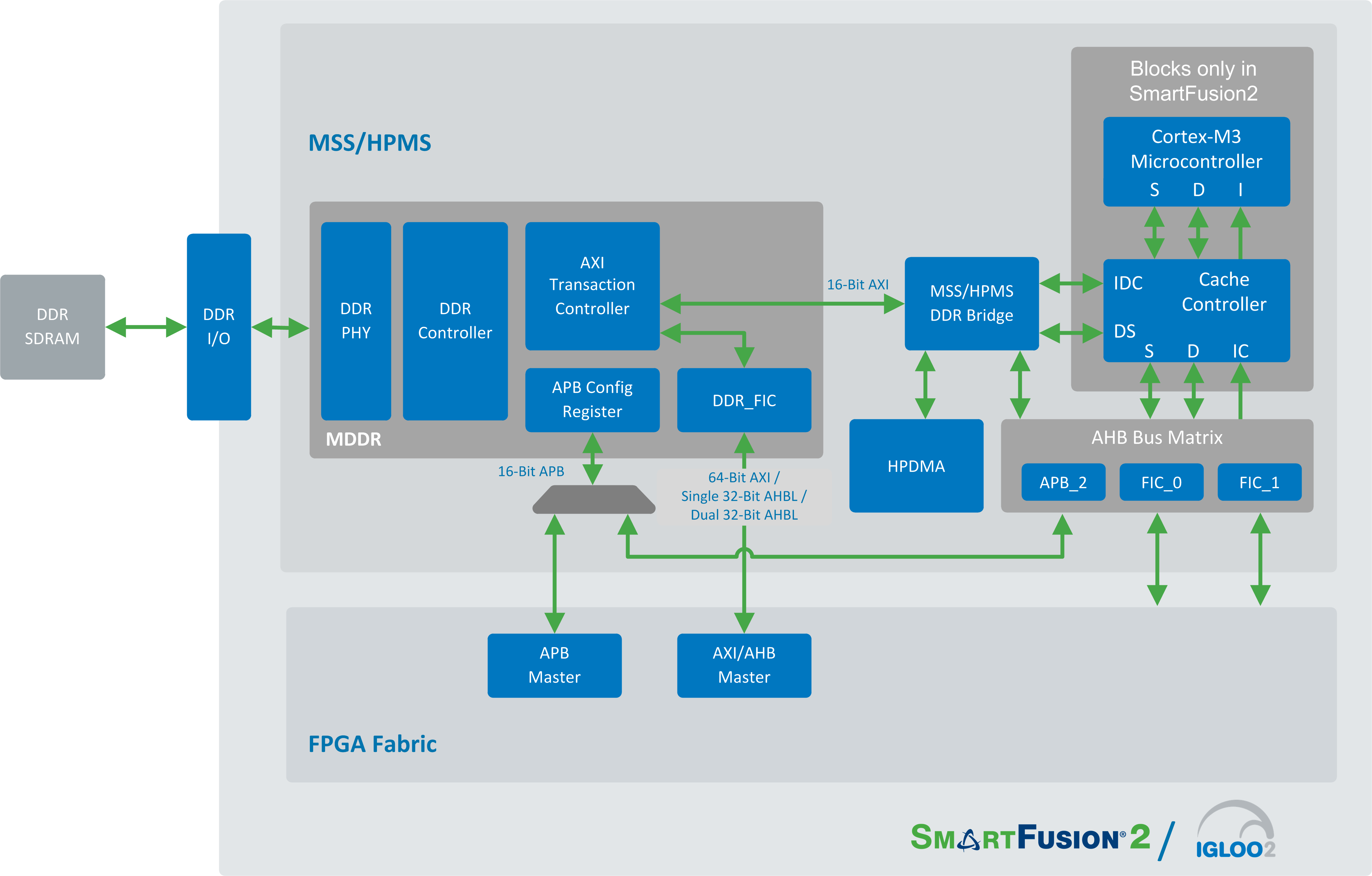
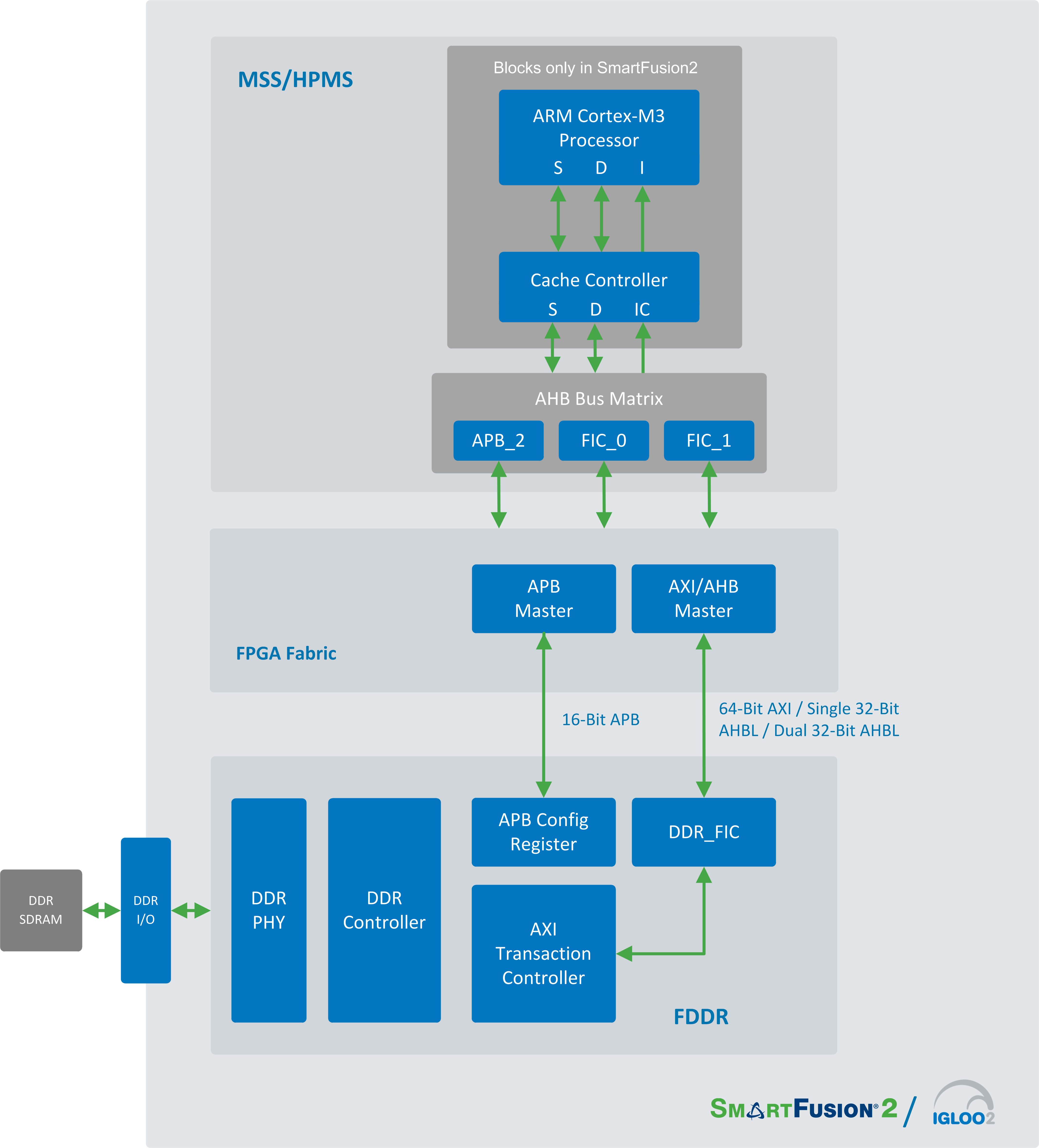
DDR Controller
In SmartFusion2 and IGLOO2, MDDR and Fabric DDR (FDDR) are two hardened ASIC blocks for interfacing the DDR2, DDR3, and LPDDR1 memories. The MDDR and FDDR subsystems are used to access DDR memories for high-speed data transfers and code execution. These subsystems include a DDR memory controller, DDR PHY, and arbitration logic to support multiple masters.
In SmartFusion2, the DDR Memory connected to the MDDR subsystem can be accessed by the MSS Masters and master logic implemented in the FGPA fabric (FPGA fabric master).
In IGLOO2, the DDR Memory connected to the MDDR subsystem can be accessed by the high-performance memory subsystem (HPMS) masters and master logic implemented in the FPGA fabric (FPGA fabric master).
The FPGA fabric masters communicate with the DDR memories interfaced to the FDDR subsystem through AXI or AHB interfaces.
Key Features
- Integrated on-chip DDR memory controller and PHY
- Configurable to support LPDDR1, DDR2, and DDR3 memory devices
- Up to 667 Mbps (333.33 MHz DDR) performance
- Supports memory densities up to 4 GB
- Supports 8-/16-/32-bit DDR standard dynamic random access memory (SDRAM) data bus-width modes
- Supports a maximum of 8 memory banks
- Supports single rank of memory
- Optional Single error correction and double error detection (SECDED) mode
- Supports DRAM burst lengths of 4, 8, or 16, depending on configured bus-width mode and DDR type
FDDR Block Diagram
Soft MC
Apart from the hard IP blocks for the commonly used memories, Soft Memory Controllers are available as IP cores for other type of memories i.e. QDR and are implemented in the FPGA fabric. Microsemi enhances design productivity by providing an extensive suite of optimised soft memory controller IP cores for use with Microsemi FPGAs and SoC FPGAs.
Soft Memory Controller
The SmartFusion2 and IGLOO2 soft memory controller fabric interface controller (SMC_FIC) is used to access external bulk memories other than DDR through the FPGA fabric. The SMC_FIC can be used with a soft memory controller for the Microcontroller Subsystem (MSS)/High Performance Memory Subsystem (HPMS) to access memories such as SDRAM, flash and SRAM.
CoreMMC
CoreMMC provides a Multimedia Card (MMC) controller to interface external MMC flash and eMMC devices. The controller allows storing boot images and booting the processor from the removable flash card. The flash card can also be used to expand the on-board storage capacity for larger applications or to store user data.
CoreQDR
CoreQDR provides a soft controller for interfacing with Quad data rate (QDR), QDR II or QDR II+ SRAMs. Quad data rate synchromous dynamic random access memories (SDRAMs) are a family of SRAMS with separate read and write channels, each operating at double data rate (DDR), optimised for high-performance communications applications such as the data plane memory of routers. QDR SDRAM performs functions such as packet buffering, statistics counting, and flow rate control.
CoreSDR
CoreSDR provides a high-performance interface to single-data-rate (SDR) synchronous dynamic random access memory (SDRAM) devices. CoreSDR accepts read and write commands using the simple local bus interface and translates these requests to the command sequences required by SDRAM devices. CoreSDR uses bank management techniques to monitor the status of each SDRAM bank. Banks are only opened or closed when necessary, minimizing access delays. Up to four banks can be managed at one time. Access cascading is also supported; allowing read or write requests to be chained together. This results in no delay between requests, enabling up to 100% memory throughput for sequential accesses.
For a complete list of memory related IPs, refer to the Intellectual Property page for Memory Controller Direct Cores.Getting Started
Software Tools
- Libero SoC Design Software integrates industry leading synthesis, debug and DSP support from Synopsys, and simulation from Siemens with power analysis, timing analysis and push button design flow.
Hardware Tools
-
PolarFire Evaluation Kit:- Microsemi offers a 300K LE PolarFire-based kit with DDR4, DDR3 and SPI-flash for a broad class of applications, that is ideally suited for high-speed transceiver evaluation, 10Gb Ethernet, IEEE1588, JESD204B, SyncE, SATA and more.
-
SmartFusion2 Advanced Development Kit - Microsemi offers 150K LE device inherently integrates reliable flash-based FPGA fabric, a 166 MHz Cortex™-M3 processor digital signal processing (DSP) blocks, static random-access memory (SRAM), embedded nonvolatile memory (eNVM), and industry-required high-performance communication interfaces— all on a single chip.
-
The SmartFusion2 Security Evaluation Kit - provides the low-cost platform to evaluate design and data security features offered by the SmartFusion2 devices. Evaluation board features M2S090TS-FGG484 90K LE device and includes various high speed interfaces like PCIe Gen2x1, four SMA connectors for SERDES, RJ45 for 10/100/1000 Ethernet. Current measurement test points have been provided to evaluate the low-power capabilities of the device. Using SmartFusion2 device features and on-board resources, kit helps in quick prototyping of low-power, secure and highly integrated applications.
-
SmartFusion2 Starter Kit - provides a cost effective platform for evaluation and development of a SmartFusion2 SoC FPGA based solution. The kit utilizes a miniature mezzanine form factor system-on-module, which integrates the SmartFusion2 device with 64MB LPDDR, 16MB SPI Flash and Ethernet PHY. The baseboard provides easy to use benchtop access to the SmartFusion2 SoC and interfaces
-
IGLOO2 Evaluation Kit provides a cost effective platform for evaluation and development of an IGLOO2 FPGA based solution.
Demos and User Guides
PolarFire SmartFusion2- DG0568: Interfacing SmartFusion2 SoC FPGA with External LPDDR Memory through MDDR Controller Demo Guide
- DG0386: SmartFusion2 Code Shadowing from SPI Flash to DDR Memory Demo Guide
- DG0669: SmartFusion2 Code Shadowing from SPI Flash to LPDDR Memory Demo Guide
- DG0618: Error Detection and Correction on SmartFusion2 Devices using DDR Memory Demo Guide
- DG0388: SmartFusion2 - Error Detection and Correction of eSRAM Memory User Guide
- TU0372: Interfacing SmartFusion2 with DDR3 Memory through MDDR Controller Tutorial
RTG4

