

ZL30252,ZL30253
3-Input, 3-Output Any-to-Any Clock Multiplier and Jitter Attenuator ICs
Overview
| The ZL30252 and ZL30253 are flexible, high-performance, clock multiplier/jitter attenuator ICs. From any input clock frequency 1kHz to 1250MHz these devices can produce frequency-locked output frequencies from 1Hz to 1035MHz and as many as 3 differential or 6 CMOS output clock signals. Output jitter is typically 0.16 to 0.28ps RMS (12kHz to 20MHz). Automatic self-configuration from external (ZL30252) or internal (ZL30253) EEPROM allows clock signals to be available immediately after power-up or reset. |
ZL30252 and ZL30253 Product Preview
ZL30252 and ZL30253 White Paper: Versatile, Easy-to-Use Solutions for a Wide Variety of Timing Challenges
White Paper: Time and Frequency Synchronization in Broadcast Video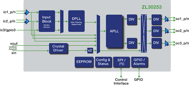
Applications/Uses
- Clocks for Processors, NPUs, FPGAs, 10G CDRs, high-speed ADCs and DACs, PCIe interface devices, Ethernet switches and PHYs
- Clock generation for wireless base stations, wireless backhaul, wired infrastructure, SONET/SDH, GE, 10G/40G/100G Ethernet, optical, storage, and broadcast video applications
Key Features
- Three Input Clocks
- Two Differential/CMOS inputs
- One single-ended/CMOS input
- Any input frequency from 1kHz to 1250MHz (1kHz to 300MHz for CMOS)
- Inputs continually monitored for activity and frequency accuracy
- Automatic or manual reference switching
- Low-Bandwidth DPLL
- Programmable bandwidth, 14Hz to 500Hz
- Attenuates jitter up to several UI
- Freerun or digital hold on loss of all inputs
- Digitally controlled phase adjust
- Low-Jitter Fractional-N APLL and 3 Outputs
- Any Output Frequency from <1Hz to 1035MHz
- High-resolution fractional frequency conversion with 0ppm error
- Easy-to-configure, encapsulated design requires no external VCXO or loop filter components
- Each output has independent dividers
- Output Jitter Typically 0.16 to 0.28ps RMS (12kHz to 20MHz integration band)
- Outputs are CML or 2xCMOS, can interface to LVDS, LVPECL, HSTL, SSTL and HCSL
- In 2xCMOS mode, the P and N pins can be different frequencies (e.g. 125MHz and 25MHz)
- Per-output supply pin with CMOS output voltages from 1.5V to 3.3V
- Precise output alignment circuitry and per-output phase adjustment
- Per-output enable/disable and glitchless start/stop (stop high or low)
General Features
- Automatic self-configuration at power-up from external (ZL30252) or internal (ZL30253) EEPROM; up to four configurations, pin-selectable
- Numerically controlled oscillator mode
- Spread-spectrum modulation mode
- SPI or I2C processor Interface
- Tiny 5x5mm QFN package
- Easy-to-use evaluation software
- ZL30253 can be ordered with up to four user-defined, factory-programmed device configurations
Resources
Parametric Search
- {{n+1}} Showing per page
| Parts | Part Status | package Type | Package Carrier | {{attribute.name | noComma}} ({{attribute.type}}) |
This category has no Parametric Data! please try other Categories