

ZL40218,ZL40219
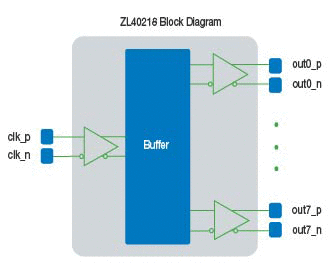
ZL40218 Precision 1:8 LVDS Fanout Buffer
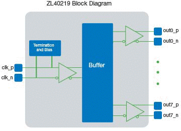
ZL40219 Precision 1:8 LVDS Fanout Buffer with On-Chip Input Termination
Overview
The ZL40218/ZL40219 are LVDS clock fanout buffers with eight identical output clock drivers capable of operating at frequencies up to 750MHz. Inputs to the ZL40218 are externally terminated to allow use of precision termination components and to allow full flexibility of input termination. The ZL40218 can accept DC or AC coupled LVPECL, LVDS, CML or HCSL input signals; single ended input signals can also be accepted. The ZL40219 provides an internal input termination network for DC and AC coupled inputs; optional input biasing for AC coupled inputs is also provided. The ZL40219 can accept DC or AC coupled LVPECL and LVDS input signals, AC coupled CML or HCSL input signals, and single ended signals.
The ZL40218/ ZL40219 are designed to fanout low-jitter reference clocks for wired or optical communications applications while adding minimal jitter to the clock signal. An internal linear power supply regulator and bulk capacitors minimize additive jitter due to power supply noise. The device operates from 2.5V+/-5% or 3.3V+/-5% supply. Its operation is guaranteed over the industrial temperature range -40°C to +85°C.
Applications/Uses
- Low jitter clock distribution
- Level translation
- Clock and data signal restoration
- Wired communications: OTN, SONET/SDH, GE, 10 GE, FC and 10G FC
- Wireless communications
- High performance micro-processor clock distribution
Key Features
- Accepts differential or single-ended input
- 8 precision LVDS outputs
- Maximum operating frequency of 750 MHz
- 2.5 V or 3.3 V power supply
- Ultra low additive jitter
- On-chip input termination resistors and biasing for AC coupled inputs
- Industrial temperature range: -40°C to +85°C
- On-chip Low Drop Out (LDO) Regulator for superior power supply rejection
Today’s modern systems often require the distribution of several clock frequencies to multiple loads. Clock buffers complement clock synthesis devices by providing additional fanout capability as needed. The ability to create multiple copies of a clock signal and distribute them among several loads with minimal additive jitter is a key advantage of a strong clock management solution. Jitter budget is mostly dedicated to the clock source and very little is left for clock management. Microsemi’s high performance buffers add minimal jitter combined with industry’s best power supply noise filtering for LVDS outputs. This results in reducing system cost and easing the design.
Resources
| Datasheets | ZL40218 Precision 1:8 LVDS Fanout Buffer Data Sheet ZL40219 Precision 1:8 LVDS Fanout Buffer with On-Chip Input Termination Data Sheet |
|---|---|
| Application Notes | ZLAN-414 Footprint Compatibility of Microsemi Clock Buffers |
| Product Reviews | Clock Distribution Fanout Buffers Clock Distribution Selector Guide |
| Downloads, Firmware and Drivers | ZL40218 IBIS ZL40219 IBIS |
Parametric Search
- {{n+1}} Showing per page
| Parts | Part Status | package Type | Package Carrier | {{attribute.name | noComma}} ({{attribute.type}}) |